German nanotechnology specialist attocube offers scanning probe microscopes to study the behaviour of complex magnetic nanostructures at ultralow temperatures

Pushing the boundaries of nanoscale imaging while embracing the extremes of ultralow operating temperatures. That’s the core value proposition offered by attocube, a German manufacturer of specialist nanotechnology solutions for research and industry, when it comes to the design, development and optimization of its portfolio of scanning probe microscopes (SPMs) and related accessories.
Despite the complexities associated with cryogenic operation, the attocube product design team is intent on bridging the gap between room-temperature SPM and ultralow-temperature applications. In short: the realization of versatile and easy-to-use SPM instrument platforms spanning a range of modalities, including (but not limited to) atomic force microscopy (AFM), conductive-tip AFM, magnetic force microscopy (MFM), piezo-response force microscopy and Kelvin probe force microscopy.
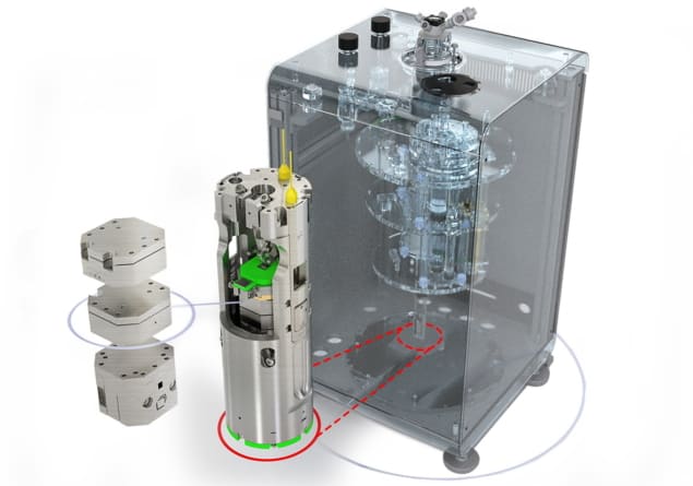
A “lighthouse customer” in this regard is Stuart Parkin, whose team at the Max Planck Institute for Microstructure Physics in Halle, Germany, is using the attocube MFM (an attoAFM I microscope with an attoMFM upgrade in an attoLIQUID2000 cryostat) to study the physical properties of materials systems with possible applications in so-called “racetrack memories”. This early-stage technology, the basic principles of which were originally elaborated by Parkin in 2002, represents a promising candidate for next-generation solid-state, non-volatile memory devices that exploit the current-controlled motion of magnetic domain walls in magnetic nanowires.
Magnetism deconstructed
The broader commercial drivers here – ultrahigh-density storage capacity and significantly enhanced energy efficiency – are rooted in fundamental materials physics. Not least the fact that racetrack memories are innately three-dimensional – in contrast to the inherent 2D structure of both magnetic disk drives (with data stored in a single 2D sheet of magnetic material) and silicon-based microelectronics (in which logic is carried out using a single sheet of transistors fabricated in the surface of single-crystal silicon).

Right now, Parkin and his team are focused on understanding the underlying physical properties of a specific class of magnetic nanostructure – known as topologically protected, non-collinear magnetic domain walls – while evaluating their potential utility as a vehicle for fast and energy-efficient data transfer in future racetrack-memory devices. “What we want to do is image these magnetic textures down to the nanoscale,” explains Parkin. “It’s not so easy, though – there aren’t many ways to do this effectively.”
One approach that’s being pursued in Parkin’s laboratory is Lorentz transmission electron microscopy – a powerful tool to study crystal and magnetic domain structures in correlation with novel physical behaviours. The downside, however, is that this imaging modality requires the scientist to make very thin, electron-transparent laminar membranes of the sample so that the electron beam can pass through – a significant overhead in terms of research productivity and output. “Sample preparation is tricky, time-consuming and can also damage the material under study,” notes Parkin.
Positioning for success
Conversely, sample preparation is a lot simpler for cryo MFM imaging (as the grown sample just has to be glued to the sample holder and contacted electrically prior to cool-down and measurement). In terms of specifics, the attoAFM I works by scanning the sample below a fixed cantilever and measuring deflection of the latter with a fibre-based optical interferometer to reconstruct the magnetic texture of the sample surface (with a lateral resolution of <30 nm).
The microscope exploits a set of xyz positioners for coarse positioning of the sample over a range of several mm, while dedicated, mechanically amplified piezo-based xyz scanners ensure a very large scan range even at cryogenic temperatures. Crucially, the use of non-magnetic materials throughout the system means the microscope is ideally suited for low-temperature MFM applications (down to 1.8 K) in combination with high magnetic fields (up to 12 T).
“The attocube MFM gives us access to a wide operating temperature range [1.8 K up to 300 K],” explains Parkin. “Equally important, the system’s vector superconducting magnet means it is also straightforward to apply magnetic fields to our samples – whether perpendicular, in-plane or at a range of angles.” Flexibility is a given: as such, the system can be equipped with the user’s choice of superconducting magnet, be it a single solenoid, split coils or 2D/3D vector magnets (including a suitable magnet power supply and the superconducting leads).
One of attocube’s main technology differentiators, says Parkin, is the manufacturer’s “expertise and legacy” in the design and development of nanopositioning stages for sample manipulation (with the patented slip-stick principle providing several degrees of freedom over several mm and with sub-nm precision). “The attoAFM I is a versatile platform,” he adds. “What’s more, attocube manufactures the whole system, integrating the MFM head, nanopositioning stage, magnet and cryostat, and with the control software knitting it all together.”
Equally important is the vendor–customer relationship and what Parkin identifies as a collaborative model of technology innovation. “It’s clear that attocube builds products with a lot of forethought and consideration to take advantage of emerging research opportunities,” he concludes. “In this way, the attocube product development team is happy to gather feedback from end-users who might have ideas for novel instrument designs and improvements.”
Engagement is everything: listening to the end-user

Mirko Bacani is the senior product manager for attocube’s cryogenic instruments portfolio, a business unit comprising four main product lines: cryogenic nanopositioners, automated low-vibration cryostats, scanning probe and confocal microscopes, and measurement tools for “cold science”. Here he tells Physics World how the company’s mission to facilitate cutting-edge materials research “starts and ends with a granular understanding of the scientific customer’s evolving requirements”.
What does your role at attocube involve on a day-to-day basis?
I have a research background in condensed-matter physics, with specialist know-how in the application of cryo MFM to a range of problems in fundamental science. As such, I speak the same language – in fact, the same dialect – as the physicists and materials scientists using our cryogenic instruments. My job is to put myself in the customer’s shoes, so I spend a lot of time analysing trends in condensed-matter research and talking to scientists – whether in their laboratories or at conferences – to understand their technology requirements versus emerging lines of scientific enquiry. Effectively, I act as a bridge between the customer and our in-house product development teams, communicating “must-haves” from the end-user and then agreeing the appropriate technical solution and product implementation.
How does attocube differentiate itself in terms of product development and innovation?
Vertical integration underpins the attocube value proposition. We develop and manufacture all of the core building blocks in our commercial instruments, giving us full control over functionality and quality assurance at the component, subsystem and system level. In cryo MFM, for example, those enabling technologies include the nanopositioning stage, scanning subsystem, deflection detection unit as well as the microscope housing and low-vibration cryostat. That granular level of control shapes our product development roadmap and ongoing technology innovation, allowing our engineering teams to iterate advanced product features in a modular fashion and ultimately deliver an optimized product to fulfil the “workhorse” role in research labs around the world.
What about your approach to customer acquisition and new business?
Here again, we prioritize specialist domain knowledge and expertise in our front-line sales engineers, all of whom have postgraduate research experience in the physical sciences. Their role is much more than sales, though, it’s specialist technical consulting – understanding the customer’s science and their instrumentation requirements. Put simply: we don’t need to know the answers to the customer’s research questions, though we do need to understand the questions themselves. In this way, we can develop enabling technologies that will unlock the creativity, ingenuity and imagination of all our end-users. It’s an approach that works: many new customers come to us when they see the success of existing customers with attocube equipment.
So ultimately it’s all about that close engagement with the end-user?
Correct. Every cryo MFM, for example, is installed in the laboratory in the presence of the customer. That process – installation, commissioning and acceptance – takes around three days, with an exhaustive approach to product training and knowledge transfer. All part of attocube’s mission to enable ongoing scientific impact for its customers through cryogenic instrumentation.


